Tomorrow’s products rise today at the IoT & AI Insider labs
![]() Bill Briggs
Microsoft News Center Staff
Bill Briggs
Microsoft News Center Staff
Just past a secured door, a software engineer in gray sweats and a blue T-shirt deftly moves from station to station, grinding out familiar tasks on an ultra-modern assembly line. Here, he slices and solders. There, he mills and melts. By the final stop, he’s helped another customer connect another device to the cloud.
The engineer adores this well-lit space, a milieu that’s part fab lab, part micro factory. In the black ceiling above, ducts exchange the air every 15 minutes. At a workbench nearby, three colleagues pick through prototypes of device cases freshly printed from gypsum. All around, walls are lined with a laser cutter, a reflow oven, a 3D printer and other machines seemingly plucked from a developer’s sweetest daydream.
“I’m in a room with every conceivable machine I could ever want to use, surrounded by a team of experts in everything I don’t know well,” says the engineer, Sean Kelly. “I can build anything I want to build. Then, you bring in customers with a problem and we get to solve it. For an engineer, it’s the closest thing to nirvana.”
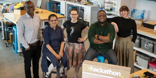
Welcome to one of Microsoft’s IoT & AI Insider labs, where engineers like Kelly help guests elevate their businesses and products by tapping into the Internet of Things and artificial Intelligence, further fueling a transformation across sectors that range from energy to retail to robotics.
The newest lab, which Microsoft will open in April in Munich, joins two others launched recently by Microsoft in Shenzhen, China, a hardware hotbed, and in Redmond, Washington, where Kelly works. Munich, an industrial hub of machinists and manufacturers, offers a location that is a central point for interested lab customers in Europe and the Middle East.
Companies of all sizes can work in the labs at no cost. They get access to Microsoft technology and its engineers’ expertise in machine learning, AI and the cloud, all in one-stop shops. During stints that typically span from one to three weeks, visiting development teams learn how to refine their product architecture, unblock technical issues and build the skills to create a full-stack IoT solution.
Four-person, full-time teams of engineers versed in custom hardware, embedded software, industrial design, secure telecommunications and cloud development walk invited guests through sprint planning, tooling and testing – tasks that typically require a company to pay six or seven vendors. Ultimately, the labs help large enterprises and tiny startups alike scale and accelerate their IoT solutions to market.
“Companies have said their three weeks in the lab was worth four, five or six months of coding on their own,” says Cyra Richardson, Microsoft general manager of IoT business development.
Exploring the Redmond IoT & AI Insider lab’s three distinct rooms – and the inspirations behind the names of those spaces – provides a full flavor of the lab experience.
The Marie Curie Room
In here, atop concrete floors, it’s all about the build, the hardware and the impressive gadgetry perched against the walls. For safety’s sake, the entry door has an extra layer of badge security, and lab employees must accompany visitors.
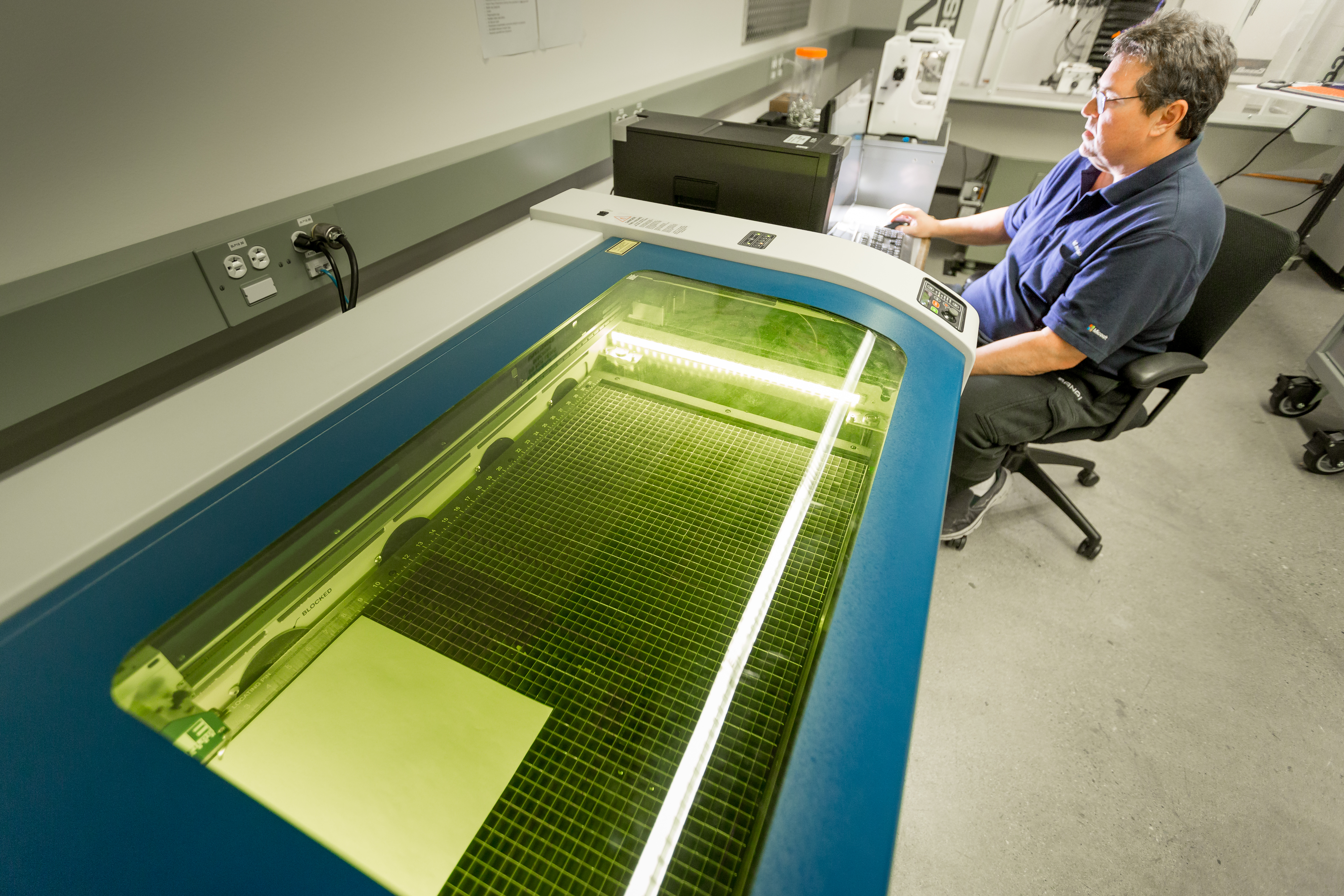
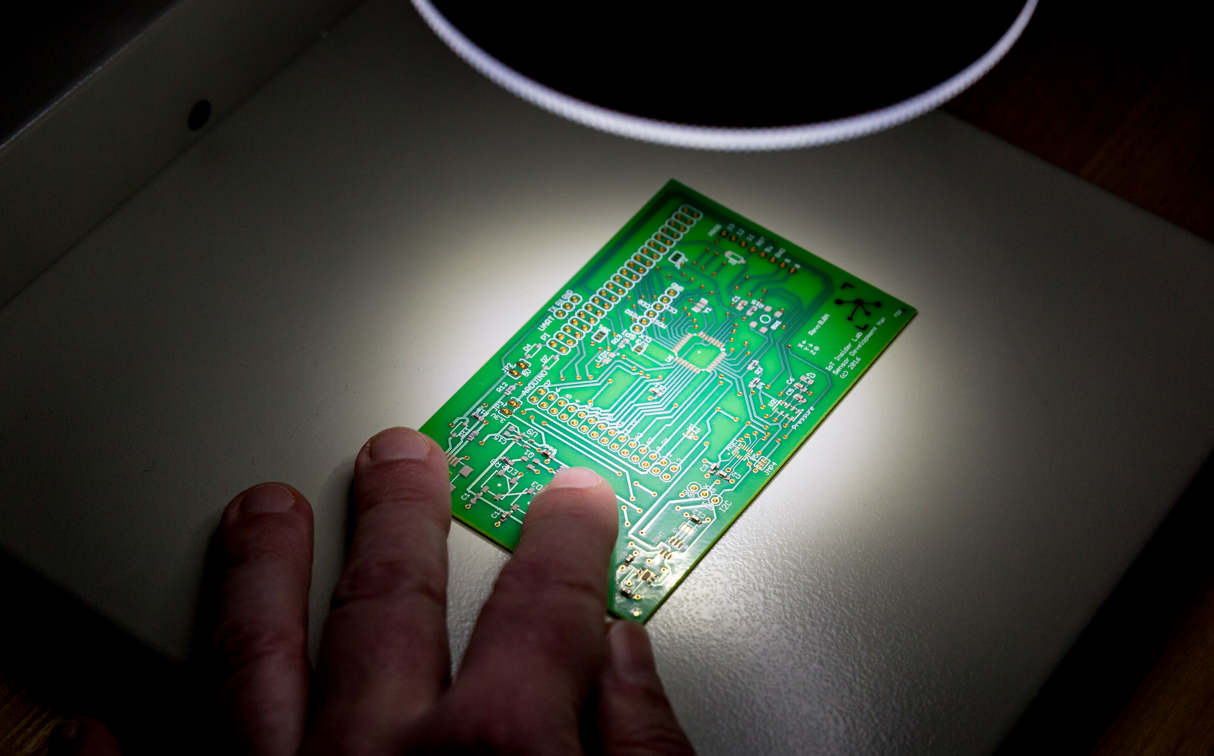
First stop is a pick-and-place machine, which mounts tiny components like circuits and resistors onto printed circuit boards – a 10-to-15-minute process.
“You can make a custom PC board, take solder paste and spread the solder paste over a stencil to deposit it at the right spots on the board. Then you take the boards out,” Richardson says, carrying several boards in one hand to a machine just to her left. “You put them in this reflow oven and this melts the solder slowly, and cools it slowly, so the components don’t fail. And then you have a working board.”
She strolls next to a full-color 3D printer. She grabs a newly made prototype for a device case, about the size of a smart phone. It’s lightweight, gritty in feel, off-white in color.
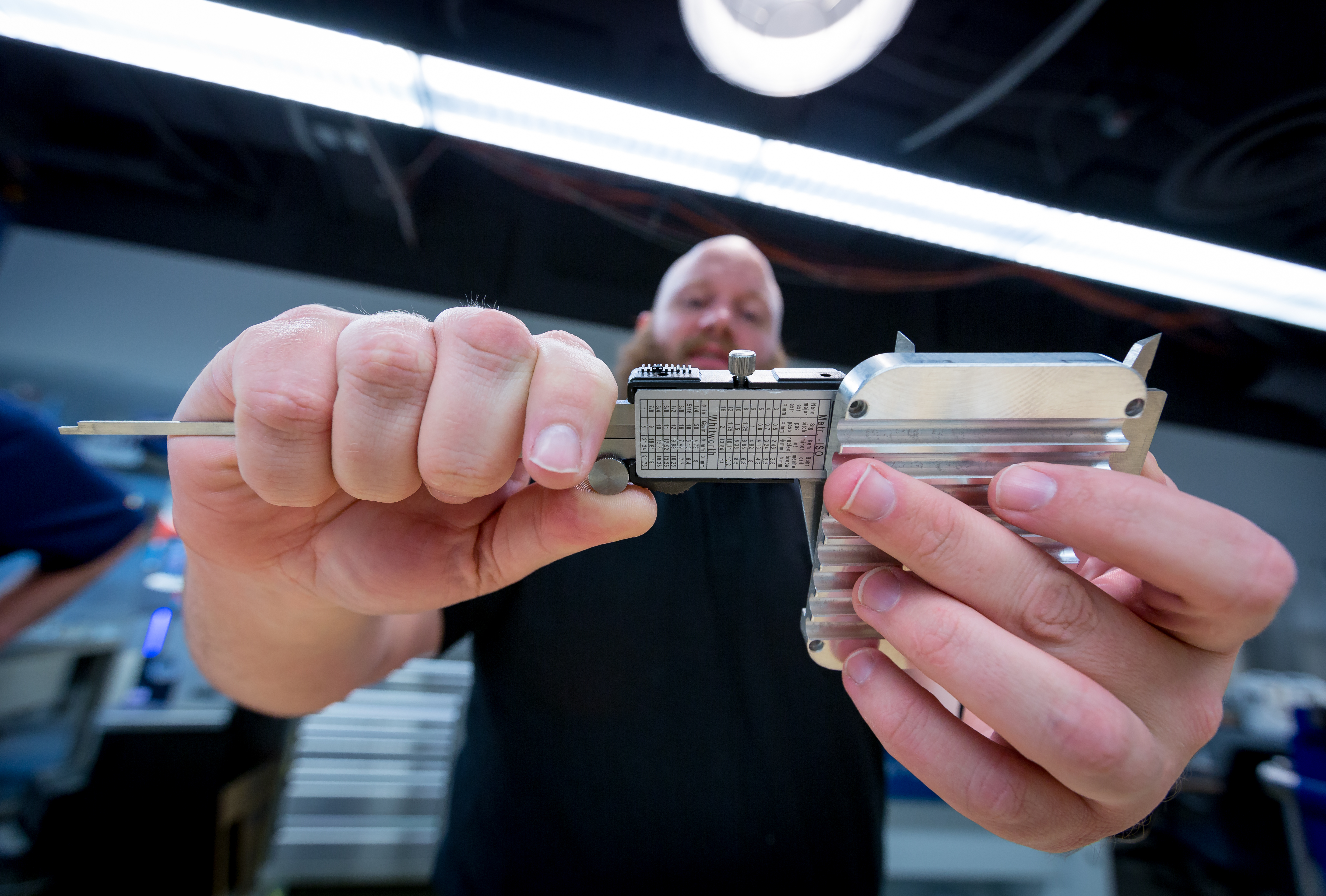
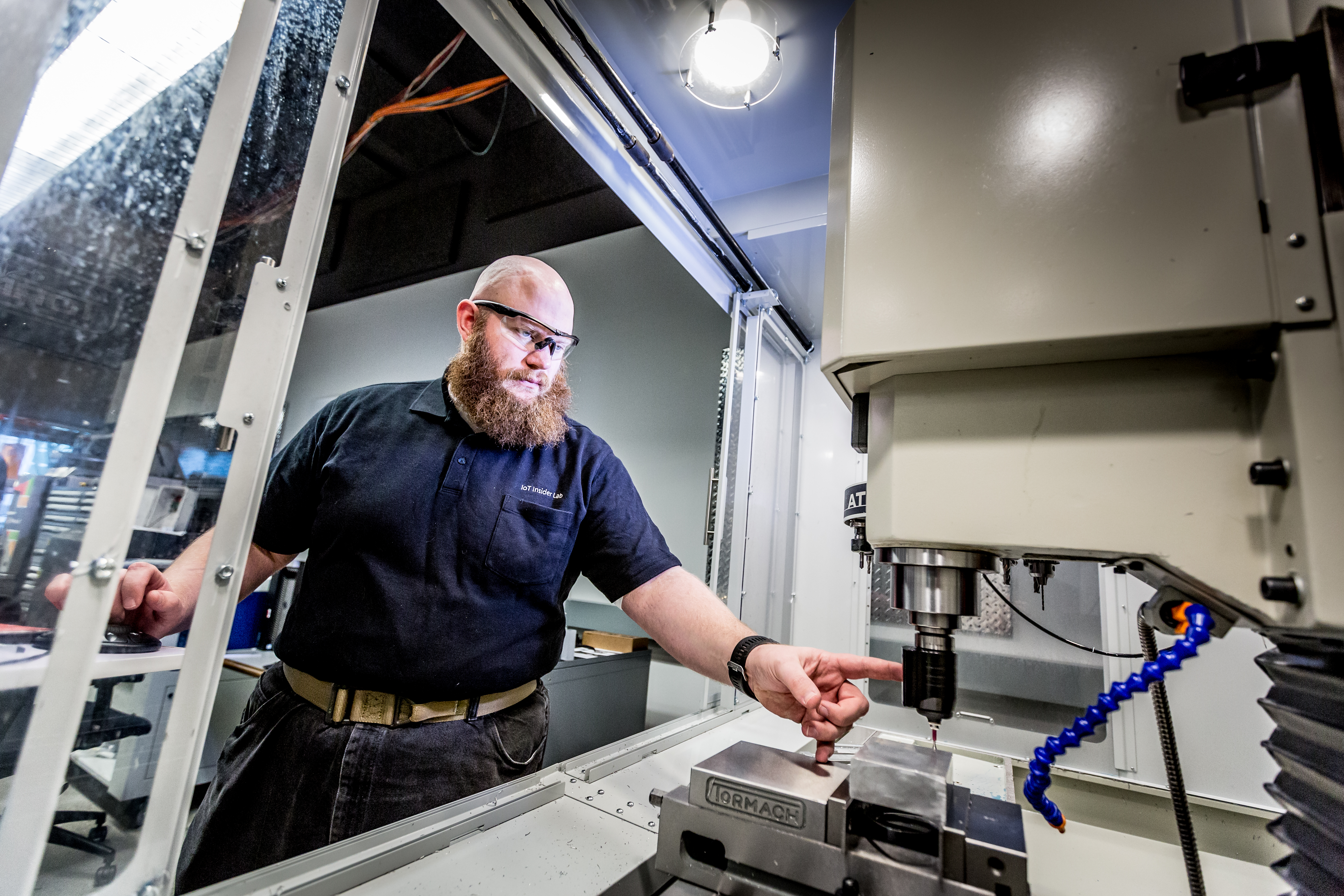
“Here’s an example of what you get out of the printer – this case is gypsum. This is not hardened yet. We’ll dip it in epoxy to harden it. You can take the same design and cut it out of aluminum in this milling machine (nearby), so now we’ve got an industrial metal case.
“You can go all the way around this loop of machines. I went from PC board, parts placement, reflow oven, 3D-printed prototype enclosure to finished metal case,” Richardson says. “Think about this: If you’re not in here, you’d have to create the schematic for the board, send it out and wait two weeks before a few boards come back. And that’s just for the PC board.”

The room’s name links the historic accomplishments of Marie Curie with the futuristic work happening now in the lab. The first woman to win the Nobel Prize, Curie was a physicist, focusing on the physical world. Fittingly, this space has a raw, industrial feel. Here, staff and customers work with their hands.
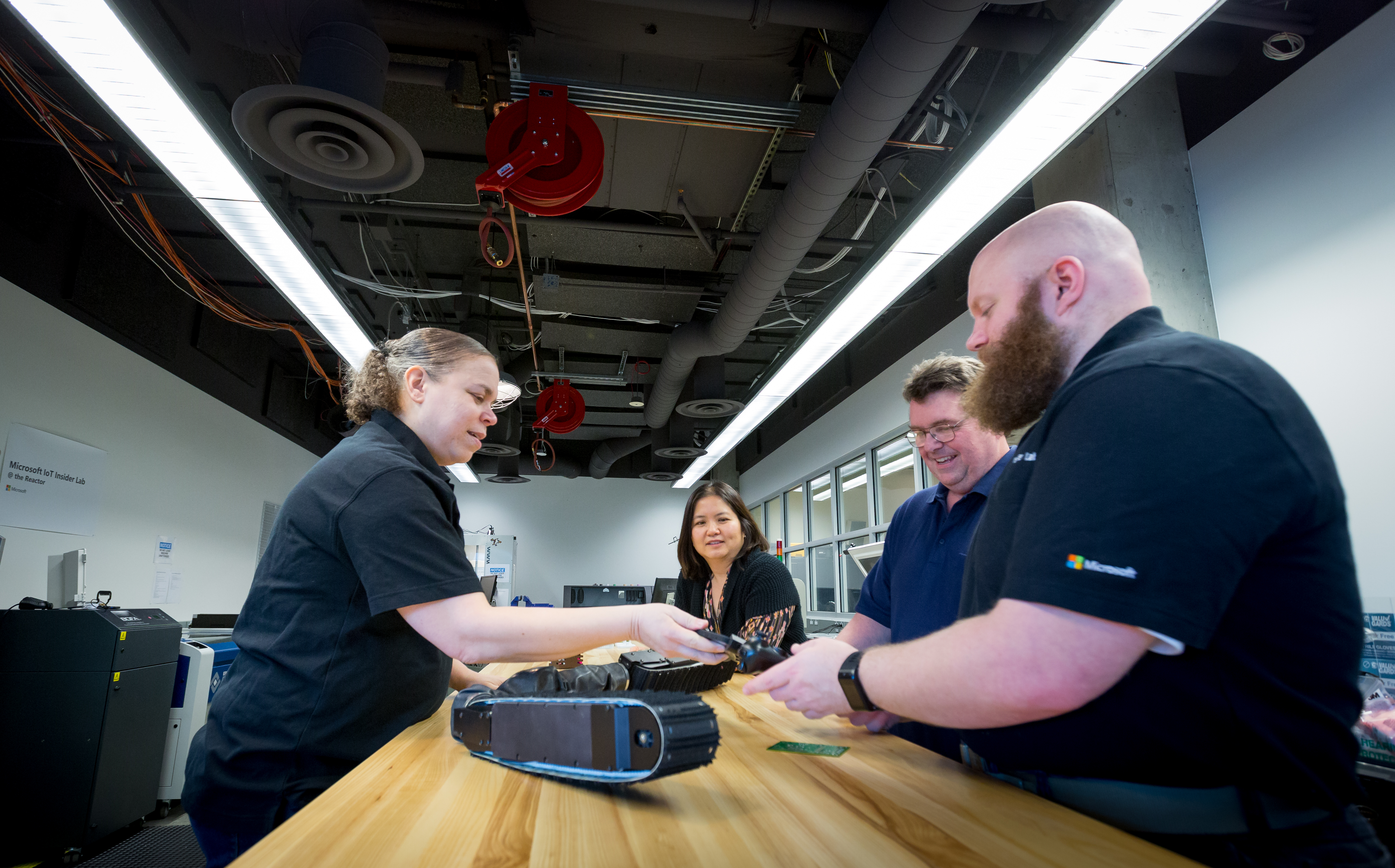
Splitting the center of the space, a long, wooden bench is strewn with stray hand tools – a wrench, a sanding block, a screwdriver. Red hoses hang from ceiling spools for customers needing air-powered tools for robotics work.
Other tools and traditional supplies sit on a corner shelf – a hacksaw and wood glue. Those remain from a recent side project. In their rare, spare minutes, some of the employees, including Kelly, tinkered with a facial recognition project for lab personnel. It hints at the innovation being nurtured here.
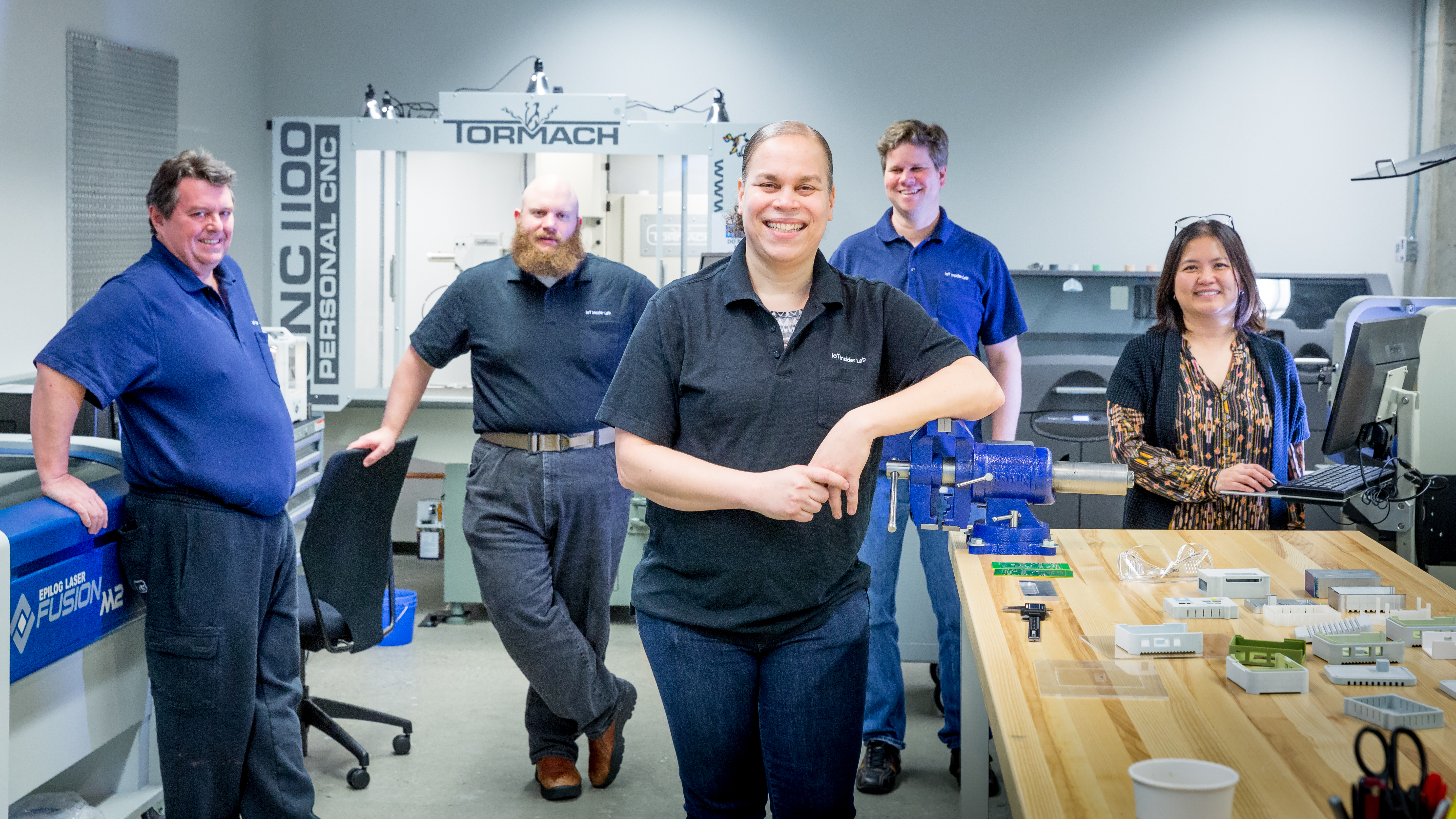
Each of the four engineers boasts a special tech proficiency, and together they represent 80-plus years of experience. When brainstorming customer problems, all ideas are valued, all voices are heard. Customers who have come through the lab have complimented the small team for its tight collaboration and ability to bounce from the needs of a shipping company to those of a retail startup.
“I’ve teased Cyra that she built this job for me,” says Kelly, who took his first job at Microsoft in 1994. He joined the lab last summer, just before the first customer arrived. “This is what I would do at home if I didn’t work here – I would get up every day and play with computers.”
“The other engineers and I have joked: We’ve got the hardware wizard, we’ve got the cloud ninja and, I guess, I’m the software sorcerer,” Kelly says.
The Ada Lovelace Room
The concrete flooring changes to carpeting as soon as Richardson walks through the next secured door that seals off the Curie Room. A wall of framed glass windows enables visitors to look back at the machine work happening there.
“Imagine taking our PC board out of the Marie Curie room and testing it in here,” Richardson says.
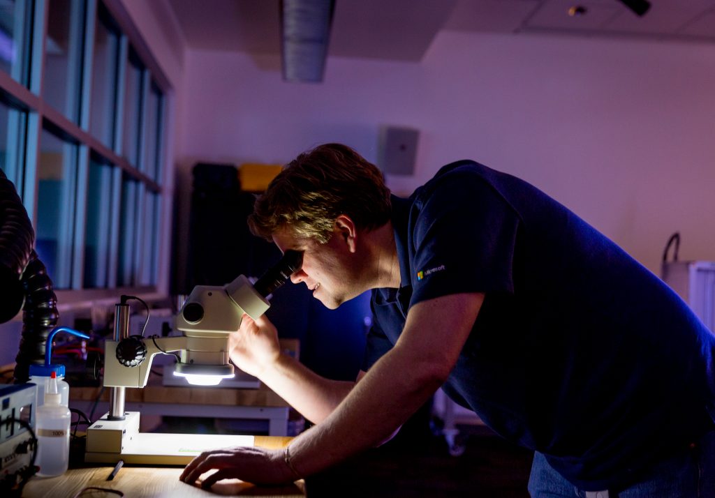
A hot-air soldering gun sits next to a microscope where participants can inspect the chips, resistors and other components on their boards. At the next station, engineers hook their boards to an oscilloscope to check individual circuit pieces.
“We have everything you need to test your product,” she says. “The Ada Lovelace room is all about coding. In here, you’re creating firmware, potentially writing the code to connect your device to Azure, and we have engineers to help you do that.”
Which explains the name. Lovelace, who lived in the first half of the 19th century, was the world’s first computer programmer.
Some of the testing work in this room involves a small chamber that measures the radio frequency strength of a device’s wireless signal. This feature helped save one lab customer, an Australian software startup called PiCo, from a costly hardware mistake.
PiCo builds and offers a point-of-sale hub that plugs into a cash register next to a barcode scanner. It serves as an automated coupon-clipping assistant, collecting real-time sales information on each customer’s purchases, letting shoppers take advantage of promotions delivered in the checkout aisle while enabling merchants to track live sales. It’s connected to the Azure cloud and presents all that data in Power BI.
In January, PiCo co-founders Andrew Lowe and Tony Nguyen entered the lab for a two-week sprint to gain comprehensive knowledge of the Azure platform, learn best practices around security, and prepare their own retail platform for scale.
Two weeks in the lab was the equivalent of about six months of product development time for us.
“It’s a great operation for a cash-strapped startup not to have to go buy all of this equipment so we can actually test what we’re building really quickly, and then turn around and make quick decisions on changes,” Lowe says.
Case in point (literally): Lowe and Nguyen brought their PiCoHub into the lab. The cloud-connected device was built inside an aluminum alloy case – a nice, clean look. They used the radio frequency chamber to assess the hub and were stunned to detect a glaring design flaw – the metallic cover blocked three quarters of the Wi-Fi signal from escaping the case.
“Instantly, within 24 hours, we knew that was not the path we wanted to go down,” Lowe says. “The lab team worked with us on the case, and we’re going to market with a plastic version as a result of that testing.”
The savings?
“Tens of thousands of dollars – which for a startup is a lot of money,” Lowe says. “I’d suggest the two weeks we were in the lab was the equivalent of about six months of product development time for us.”
Indeed, participating companies are drawn to the labs because they help reduce risk, Richardson says. Companies can apply online. Lab organizers then schedule them carefully to safeguard their intellectual property and ensure that there are clear objectives.
“For program managers, this makes it concrete enough so they can feel like their product is done – it doesn’t become a science project that goes on forever. For business decision makers, they see how they can reduce risk for their project,” Richardson says. “And for the sales teams that come through here, they get excited because the customer sees us investing in their success.
“The customers are getting assistance they couldn’t get otherwise, and from a single organization or facility. There are no other IoT labs in the world where they can get hardware-to-AI help, all under one roof,” Richardson says. “We help organizations realize their vision – and in the process generate some good will.”
The Mae Jemison Room
For the final stop on the tour, Richardson walks past a sliding wall affixed with whiteboards and steps into the lab’s third space.
This is the most dressed-up of the three rooms, with the most corporate sheen. A cluster of cushy chairs surround a glass coffee table – a spot where the lab’s engineers and visiting company participants share their morning chats to discuss what was accomplished the day before and what will get done that day.
Against one wall, three 70-inch monitors stand in a tight row.
Richardson stops by the first screen.
“The idea here would be to take your device, plug in your data, and then we look at your data and clean it,” she says. “On the next display, we look for correlation and insights. And then on the last station, we show customers how to operationalize the insights they’ve discovered.”
On a recent afternoon, the area was repurposed to demo a digital sign prototype made by the IoT Lab team for a Chinese manufacturer. In the past, smart signs have long been read-only surfaces used to display ad campaigns. In the lab, the engineers worked with the company to add a camera and Microsoft Cognitive Services to track the number of onlookers (plus their genders and approximate ages) and to read their moods as they absorbed the messages. The observer data is served up on a dashboard next to the smart sign to show how even signs can be digitally transformed into a new product and new business that sells ad impressions instead of just screens.
“The labs work with customers from a depth perspective – we unblock them and help them develop solutions for products,” says Marlina Hales, Microsoft manager of IoT business development. “We also work with lab participants from a breadth perspective, creating products to share with the community. For example, we believe in the need to nurture the next generation of developers. One of the ways we do that is through STEM in high schools and colleges,” Hales says.
Last summer, Hales teamed with an educator in rural Texas to hold a hackathon for more than 200 students who used Microsoft IoT technology to create cloud-connected devices that talk to other devices. Their partner in the project was the woman who dreamed up the event, Rafranz Davis, executive director of professional and digital learning at Lufkin Independent School District.
“During our call with Rafranz, we said, ‘Hey, we just want to help you. If we think about disadvantaged students as not having equal access to this technology and us making that access possible, it makes us feel really good to be able to inspire the next generation of developers,’” Richardson recalls.
Davis hosted the July hackathon in a cleared-out high school cafeteria. Every student participant received an Adafruit Raspberry Pi 3 Kit. Their inventions included a facial-recognition program that could log kids into the district’s attendance database, and a classroom emergency notification system that could alert school employees or local police officers, depending on the nature of the situation.
“From my journey in teaching, I know there are plenty of kids who take things apart and put things together. They look at the world and they ask questions, or they look at us and ask questions,” Davis says. “If students can actively ask questions and seek answers and build and break and fail and rise, we’re impacting them in ways we never before realized.”
That sentiment matches the inspiration behind the name of the lab’s third room. Mae Jemison, a physician and engineer, was the first African-American woman to travel into space, orbiting Earth in 1992 aboard the Space Shuttle Endeavour.
“Mae Jemison was reaching for the stars,” Richardson says. “And for a lot of people, before they come to the lab, their ideas seem almost as out of reach as space.”
Photos by Scott Eklund/Red Box Pictures.